
Updated May 10 2009
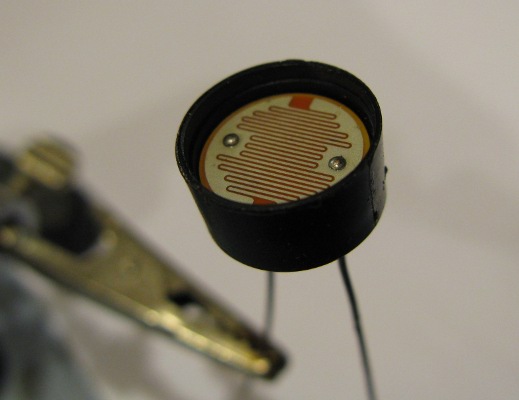
The picture above shows how transistor action was observed by improvising an insulated gate to a cadmium sulfide photo resistor. The picture was taken in normal light but the experiment had to be performed in the dark.
The photocell used is pictured above. It is a very common type which I purchased from Radio Shack many years ago.
I have long suspected that if a successful homemade transistor were to be made, it might likely happen in the form of a FET. I have read of Roger Baker's homemade FET in the June 1970 Scientific American Amateur Scientist column numerous times and have thought about the simple architecture that can make a FET. This article illustrates that a FET can be made simply by running current through a thin film of the right type of semiconductor. If a flat conductor is put very near the semiconductor film and insulated from it, voltage changes between the flat conductor and the film will cause changes in the amount of current flowing through the film.
It recently occurred to me that if this is the case, I might be able to create transistor action through a cadmium sulfide photocell (actually a photo sensitive resistor) since they consist of basically a thin semiconductor film between two electrodes. This simple experiment would be a logical first step before trying to create my own thin semiconductor films. Would this photocell act as a transistor if I put an insulated gate near it?
My first attempt was simply to observe if there is any current change through the photocell while moving a charged comb or pvc pipe near it. The excitement of seeing the current change was short lived after realizing that the light striking the photocell was also affected by the moving comb. I needed some light in the room to watch the meter. Several years ago I had also tried moving a charged comb near some catwhisker devices to see if the current changed. Seeing some current change at that time, was exciting until I realized that the electrostatic attraction from the charged comb was physically pulling on the catwhisker. I have long wondered if simply putting a charged object near a semiconductor or other type of film, could have an effect on electrical current flowing through the film. For now, that question still remains unanswered.
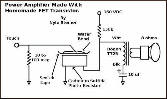
It was time to try improvising some kind of conductive gate near the surface of the photocell. I did this by putting a piece of scotch tape across the face of the photocell to act as the insulator. To make a conductive layer in close contact, I then put a drop of water on top of the scotch tape just big enough to cover most of the photocell area. I used water because of it's ability to conform closely to the surface of the tape. Nothing needed to be added to the water because the resistance of normal water is very low compared to the almost infinite resistance of this improvised gate. A piece of wire touching the drop of water served as the gate electrode.
From my observations, the setup described above definitely produces transistor action. This experiment had to be performed in the dark for obvious reasons although I found that a tiny bit of light falling on the photocell could sometimes improve performance. There was little or no transistor action in normal light because the photocell was saturated.
This transistor has considerable power gain but very low voltage gain because of the wide voltage excursions required at the gate to produce a significant current change through the photocell. Intuition says the gate could be made more sensitive by putting the gate closer but the thickness of the scotch tape and the clear coating on the front of the photocell precluded this. The gate input resistance is for most practical purposes, infinite. The only current that flows through the gate is whatever current can leak through a piece of scotch tape.
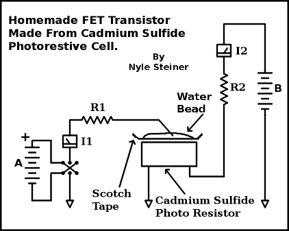
Battery B supplies current through the photocell and R2. Current through the photocell is measured by I2. Battery B was varied between 9 VDC to 175 VDC.
Battery A was varied between 75 VDC and 175 VDC and was connected through a switch to be able to reverse the polarity of voltage applied to the gate.
Whenever the switch was changed, the polarity of voltage across the gate would reverse, resulting in a current change through I2.
R1 and R2 were used mainly to limit current and protect the current meters in case of a high current. Since the gate impedance is so high, R1 could be anywhere between zero and 10 meg without noticing any significant difference.
This device acted as an enhancement-depletion insulated gate FET. A positive voltage applied to the gate caused an increase of current through I2 and a negative voltage applied to the gate caused a decrease in current through I2.
The gate, being such high impedance, is what makes the power gain of this device so high. A change of even several hundred volts across the gate usually causes at most a small fraction of a microamp - barely perceptible needle movement on a 50 ua full scale ammeter I1. This translates into a very small change of power dissipated in the gate circuit. This voltage change on the gate can cause many microamps of current change through the photocell. That translates into a significant change of power dissipated in the output circuit across R2.
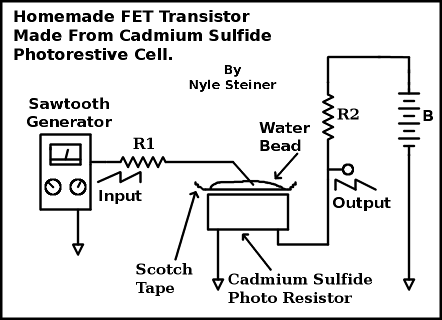
The response of this device also seemed to have a dynamic characteristic. That is, whenever the reversing switch was activated, the current through R2 would suddenly change and then slowly creep back toward the previous value. By running a sawtooth waveform into the gate however, I was able to establish to my satisfaction, that indeed the output current was responding to the input voltage.
The sawtooth waveform at the output across R2 was inverted. This provided additional assurance to me that this experiment was indeed producing real transistor action. The input and output waveforms can be seen in the pictures below. The output waveform was at much lower amplitude even though it appears the same in the lower picture. The oscilloscope gain was set higher to compensate for the lower output.
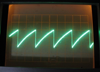
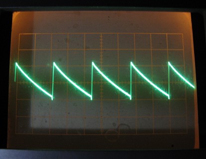
The tiny spike at the bottom of the waveform is a small amount of input signal feeding directly to the output through stray capacitance.
Meter readings and oscilloscope signals are great for evaluating devices such as this homemade transistor but, evaluation would not be complete without building an actual amplifier circuit and attempting to hear an amplified signal. I was successful at doing that.
A large voltage swing is required to drive the gate of this crude transistor. This makes it unsuitable for amplifying small voltage level signals. A weak but large voltage swing (very high impedance) signal is more suitable for driving this homemade transistor amplifier. Fortunately, this type of signal is very handy at our fingertips. The 60 HZ buzz that our bodies pick up around the house is just such a signal and is perfect for testing this amplifier.
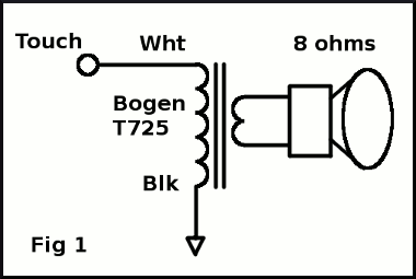
In order to make a comparison between the unamplified signal and the amplified signal, I used the circuit shown in Fig 1. When touching the "Touch" point in Fig 1, the 60 HZ buzz can just barely be heard by putting the ear right on the speaker. When touching the "Touch" point of the amplifier circuit, the buzz can be easily heard by just sitting near the speaker. Even though the signal from the speaker is still soft, the increase in loudness can clearly be heard. We usually don't care much to have a signal like this amplified, but it is very exciting to hear it amplified in this situation.
The homemade transistor requires a slight amount of light for optimum operation.
The 160 VDC is normally positive but the amplifier seemed to work just as well when the 160 VDC was negative. With the negative voltage, I had to reverse the 10 uf capacitor.
Even though the voltage gain of this circuit is very low (so far about 1/10), the power gain is considerable and I believe this experiment definitely demonstrates transistor action from a simple homemade field effect transistor. This experiment with a photocell is a positive first step. It is fascinating to think about trying homemade thin films, and the results that might be obtained, as Roger Baker did in 1970..